Our research focuses on leveraging the unique properties of nanomaterials for applications like wearable electronics, tunable nanoelectromechanicaly systems, mechanically reconfigurable quantum materials, biosensors, and new energy systems. Our research explores using molecular scale building blocks made from new 2D materials like graphene and molybdenum disulfide to re-engineer classic 3D systems at atomic length scale such as atomically-thin membranes or flexible films and electronic structures such as transistors and photodiodes.
2D membrane mechanics & NEMS
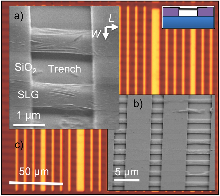 What can we do with a sheet of paper only one atom thick? By taking advantage of the outstanding mechanical properties of 2D materials, we are building new Nanoelectromechanical systems out of atomic membranes, with with a focus on applications in signal processing, sensing, and flexible, reconfigurable, electronics.
Scalable Synthesis of new 2D materials
 The first step to making 2D materials a technology is developing reliable and scaleable methods for producing high quality films. While graphene, a sheet of carbon only one atom thick, is the most famous example of a 2D material, there are actually hundreds of members of of the family with wildly different properties, giving a diverse pallet to explore nanoscience in two dimensions. We are working on methods to grow any 2D material for use in devices and applications.
Impact of nanoscale defects
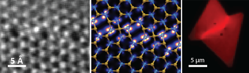
The quality of any material is usually limited by the type of defects that can exist. As atomically thin sheets, even having a single atom out of place can strongly affect the quality of materials. By applying an array of characterization methods, we directly correlate the structure of atomic scale disorder such as substitutional defect, grain boundaries, anisotropy, and stacking misalignment on the micro to materials and device properties on the microscale such as electrical conductivity, mechanical strength and optical absorbtion.
Nanoscale devices and band engineering from tailored 2D heterostructures
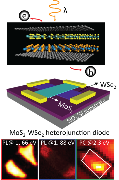 By mixing and matching 2D materials as nanoscale building blocks, we can re-engineer many electronic, photonic and mechanical device at molecular length scales. However, because a 2D monolayer is, by definition, all surface, the individual layers in a heterostructure no longer behave as independent building blocks. Many properties, from thermal expansion coefficient, to electronic band structure, to interlayer energy transfer will depend on the exact structure of the interface. We take advantage of this fact to engineer completely new metamaterials and devices by engineering the alignment and layer number in heterostructures.